
4DScanner2
SCROLL
SCROLL
ROLE of THE PRODUCT
Product Role
Visualization of Warpage
and Flatness
in the Reflow Process
Warpage and flatness of the SMT components and the board due to heat in the reflow process cause SMT defects such as open, crack, and head-in-pillow defects. The cause of these SMT defects cannot be found only by simple inspection before and after reflow, which leads to poor yield and outflow of defective products. Therefore, it is necessary to analyze the warpage/flatness for each temperature with respect to the solder thickness. 4DScanner 2 reproduces the temperature environment of the reflow environment and visualizes the warpage and flatness of the SMT components and board during heating, allowing you to know the cause of SMT failure.
SMT defects to solve

Open
It occurs when the terminal and solder are not in contact at the solder freezing point.

Crack
Occurrence of stress due to increased warpage and flatness after the solder solidification point.

Bad pillow
Warpage and flatness increase before solder solidification point, causing solder oxidation.
Visualization

Factor
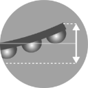
Warp
Visualize the amount of deformation of the board, IC package, and connector housing due to heat.
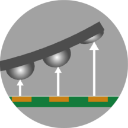
Flatness
Visualization of the floating amount of IC and connector terminals the board surface.
CONCEPT of THE PRODUCT
Product concept
4D=3D+ C
C
Change in
heating shape
3D movie analysis
It is an accurate measurement result that reproduces the reflow environment, an element necessary for the Reflow simulator, but it is just information. Testing the hypothesis for SMT failure is the goal behind the measurement.
4D of 4DScanner 2 means 3D and temperature. By making it possible to analyze the heating shape change in the reflow process with a 3D movie, you can make imagination a reality and make intuitive decisions. This narrows down the path to improvement of SMT defects and leads to problem solving with the minimum necessary approach.
VALUE of THE PRODUCT
Product value
From micro bumps to substrates
Measure with one unit
200mmの基板から 50μm の極小BGAバンプまで多種多様なSMT部品に対して、複雑なセッティングなしで 1 台で測定可能です。
Shiny to matte
Without spraying things
高輝度ブルーレーザーによる光切断法を採用することで高い測定能力を実現。ライン上の高輝度ブルーレーザーをサンプル表面全体にわたって走査する事により、位相シフト法等の光パターンを周期的に投影しての測定では、光沢を抑えるスプレーコーティング等の前処理無しでは測定が困難であったシリコンウェハー等の光沢の強いサンプルの測定も可能に。
Not only the result
Factor analysis
In addition to the flatness of the terminals, the bending of the housing can be analyzed with a realistic 3D video,Analysis of causal relationship between terminal flatness and housing warpageIs possible.

Not just heating
In reflow environment
Instead of heating on one side with a hot plate or halogen heater, use the same hot air as the reflow furnace Convection heating To reproduce the reflow environment.
Click here for details
Product review information
Available online
cores Lab is, CORES is a lab where you can experience the products.
Please feel free to contact us as we can carry out our own sample evaluation or send it online for remote evaluation.